The LHC program will define the high-energy frontier of particle physics until the end of the 2020s. Several update and upgrade steps of the accelerator are planned before then to further increase the collision rate and the energy range. In the course of these upgrades, the specifications of many components in today’s ATLAS detector will be exceeded. The Inner Detector, in particular, will continuously lose measurement accuracy as higher event rates and track densities cause greater radiation damage.
Around 2020, after having accumulated an integrated luminosity of around 300 fb-1, the silicon and gas detectors of the Inner Detector will reach the end of their service life and need to be replaced. This renewal is intended to ensure the measurement accuracy will be sufficient for the next operational phase of the LHC. The plan is to use an Inner Detector which is based purely on silicon.
In contrast to today’s detectors, the new detector will have to have low-cost pixel modules with a minimal material budget, a larger relative active area, and higher granularity. Furthermore, the modules must be able to withstand received fluencies of up to 2x10¹⁶ neq/cm2 (1 megaelectronvolt neutron equivalent). The MPP group is focusing on the development of a novel pixel module concept to be used at the so-called HL-LHC after all upgrade steps have been completed.
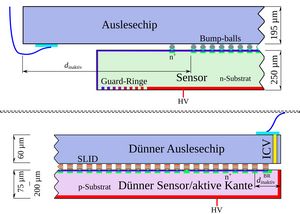
The pixel module concept meets the aforementioned requirements. Five novel technologies are employed: n-in-p pixel sensors, thin pixel sensors, narrow edges with and without implantation at the sensor edges, and a 3D-integration of sensors and read-out electronics. One 3D integration technology investigated comprises a new interconnection technology, called Solid Liquid InterDiffusion (SLID), as well as Inter-Chip Vias (ICV). The diagrams on the right show the module concept currently in use and the concept which has been investigated.
n-in-p Pixel Sensors
For n-in-p sensors, a p-type silicon substrate is used instead of the n-type silicon substrate used to date. Since the depletion of the space-charge zone of the p-n junctions now starts at the front, the guard ring structure, which is used for the controlled shaping of the electric field, can be placed on the front.
The advantage here is that the back of the sensors no longer needs to be provided with a pattern; this obviates the need for expensive masks and the relative alignment of front and back, thus making n-in-p sensors cheaper to fabricate. Their properties before and after irradiation are investigated using different experimental methods, such as particle beams of known energy and species, radioactive sources and lasers in the infra-red range. The results are compared to data for n-in-n sensors currently in use.
Thin Sensors
The thinner sensor design reduces the multiple scattering within the sensor and leads to a higher charge accumulation efficiency at the same depletion voltage after irradiation. The sensors are produced either industrially or at the MPG semiconductor laboratory. A process developed at the MPG semiconductor laboratory allows the thickness of the sensors to be reduced down to 50 micrometers, i.e. to one fifth of the thickness of the sensors currently in use. The properties of thin sensors are investigated with the aforementioned methods and their suitability for high-energy physics experiments is explored.
Narrow Edges
To achieve better positional resolution, the pixel modules are brought closer and closer to the interaction zone of the proton beams. Since this now prevents the modules from overlapping along the beam axis, the active area of the pixel modules has to be as large as possible. This can be achieved by optimizing the design of the guard ring structure, on the one hand, or by implanting the sensor cutting edges on the other.
The use of activated edges in conjunction with optimized design of the guard ring structure allows the size of the inactive edge region to be reduced from 1.1 mm to 50 micrometers. Beam test measurements are used to investigate how this modified edge region affects the properties of the sensors.
Solid Liquid InterDiffusion (SLID)
Instead of the bump-bonding process conventionally used, the so-called “Solid-Liquid InterDiffusion” (SLID) process was used to interconnect sensors and read-out electronics. This process was developed at the Fraunhofer Research Institution for Microsystems and Solid State Technologies (EMFT), and offers smaller structure dimensions and a potentially lower price compared to conventional bump bonding.
Since the temperature required for the interconnection is lower than the melting point of the eutectic alloy formed in the process, it is possible to interconnect several specialized chip layers with one sensor. The active area of these pixel modules is improved further because a smaller area is needed for the read-out. This is particularly attractive in combination with Inter-Chip Vias.
Inter-Chip Vias (ICV)
Inter-Chip Vias (ICV), also called Through-Silicon Vias, allow signals to be transported through the read-out chip to its rear instead of routing the signals to the edge of the read-out chip and reading them out on the sensor side (as happens in the configuration currently in use which is shown in the top illustration). This results in a significantly more compact module design, particularly in combination with narrow edge zones on the sensor side. It also allows the vertical integration of analog and digital read-out electronics, whereby every component can be optimized individually.

